Product Introduction
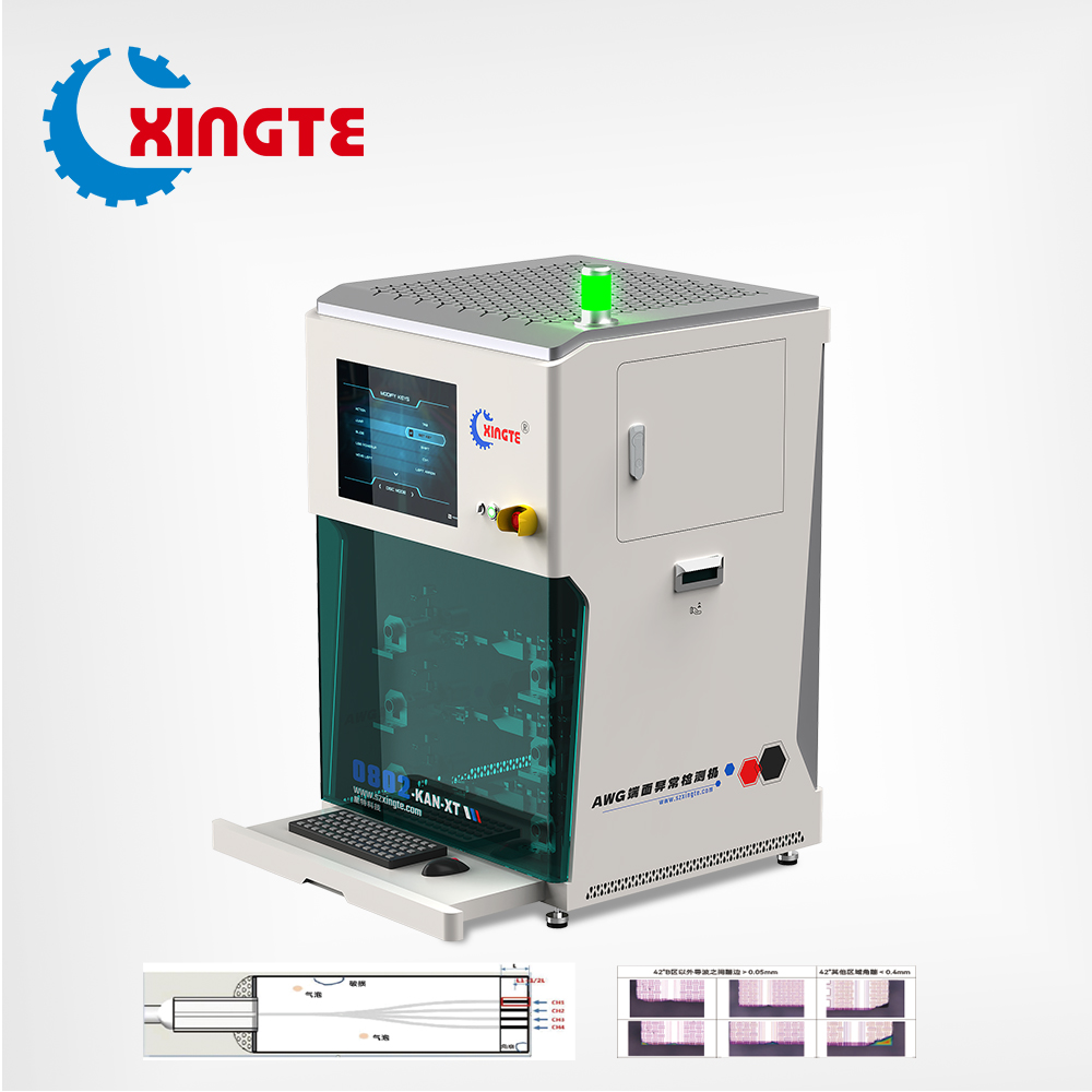
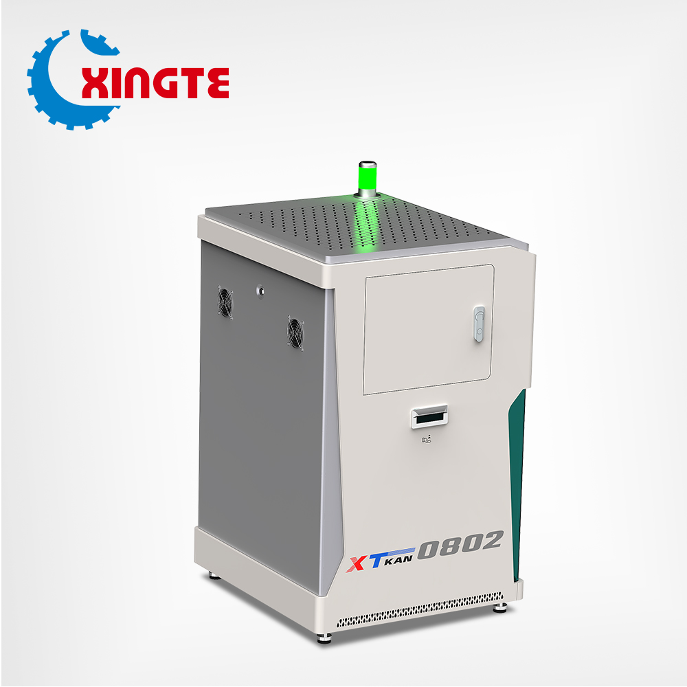
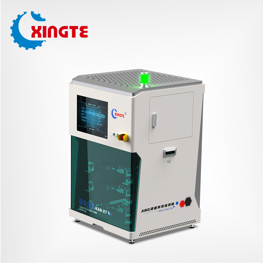
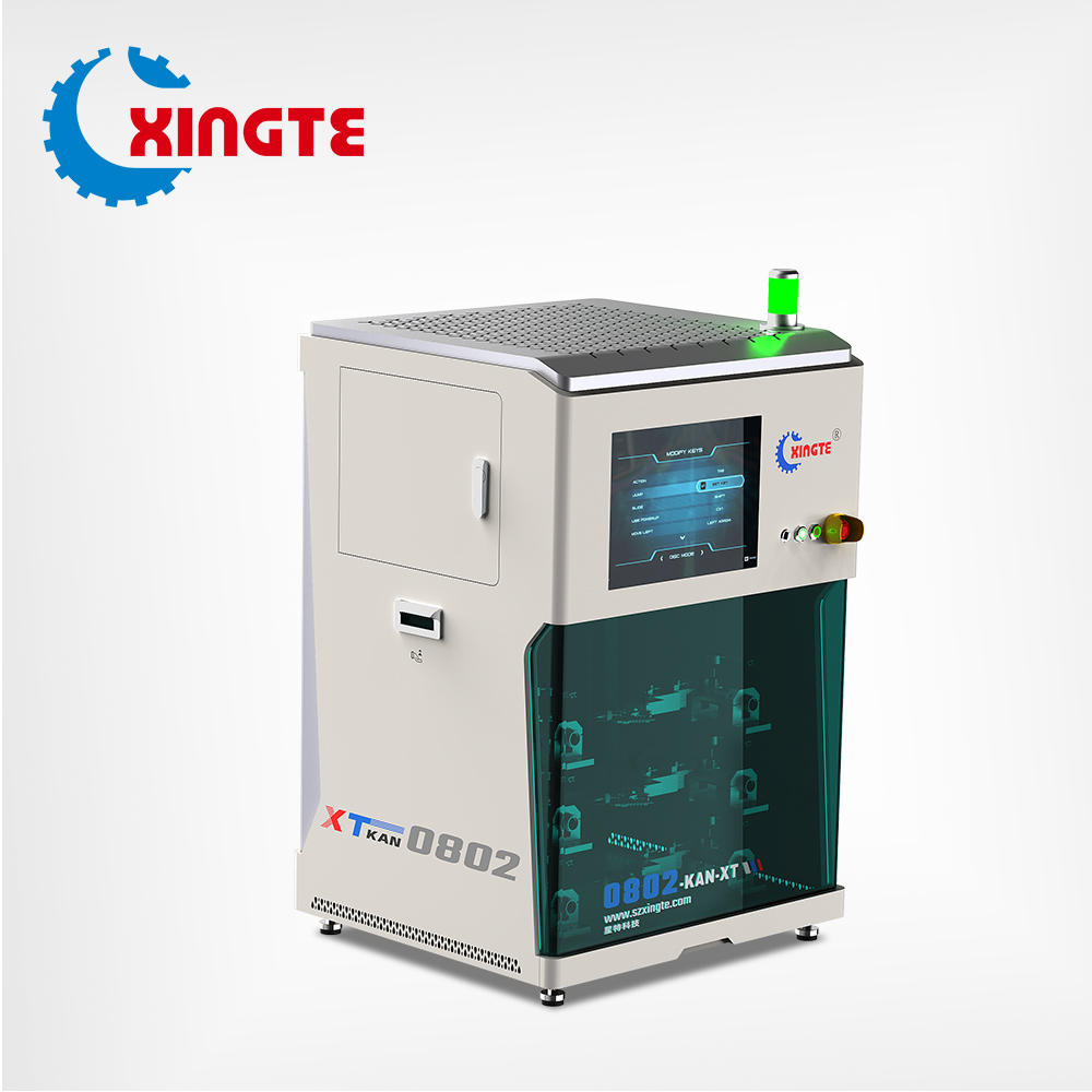
This high-precision visual inspection equipment is specially developed for AWG arrayed waveguide grating devices. Based on high-magnification microscopic imaging and AI image algorithms, it performs non-contact inspection on AWG chip end faces and waveguide channels. It identifies appearance defects such as scratches, chipping, stains and waveguide damage on end faces, and simultaneously measures key geometric parameters including channel position and spacing. Suitable for in-line quality control in mass production of high-speed optical module AWG devices. Inspection data can be stored for traceability and supports connection to the production line MES system.